Next-Generation Semiconductor Precursors and Their Challenges

Navigating the Complexities of Next-Generation Precursor Gas in Semiconductor Manufacturing
Author: Frank Horvat, PhD, Senior Scientist, Swagelok Company
Artificial intelligence (AI) grows more advanced by the day—and as a result, new demands are causing major shifts in the semiconductor industry.
Advanced AI requires greater computational density, data efficiency, thermal management, and power reduction. These trends are driving changes in global semiconductor manufacturing from major players like Samsung, Micron, TSMC, and others, as next-generation devices now demand advanced logic and tightly integrated memory to power the exponential growth required by modern AI supercomputers.
Semiconductor tool original equipment manufacturers (OEMs) have responded by introducing next-generation equipment engineered to meet evolving device specifications, while chemical suppliers continue advancing precursor chemistries and delivery technologies. Specifically, atomic scale, dielectric, conductive, and barrier films are now deposited on complex 3D transistor shapes and high-aspect ratio geometries.
Achieving uniform film coverage on these intricate shapes introduces new challenges within the atomic layer deposition (ALD) process, requiring semiconductor manufacturing professionals to continually adopt new precursor formulations to keep pace with evolving process requirements and chemistry formulations. In this blog article, we’ll examine high- and low-vapor pressure precursors, associated system design challenges, contamination and yield concerns, and how close collaboration between stakeholders will be critical for success.
Examining High- and Low-Vapor Pressure Precursors
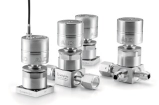
Precisely timed ALD valves that meter each pulse into the reaction chamber deliver chemical precursors used in the ALD process. The precursors react with the wafer substrate, forming one atomic layer of material per cycle. Each deposition sequence typically involves two precursor steps: a source (Precursor A) and a reactant (Precursor B). Between each source/reactance pulse, a high-vacuum purge or evacuation step removes residual gases and reactant by-products.
Due to the evolving demand of chip production, new precursors are being introduced into the marketplace to achieve new levels of performance. Depending on their behavior, they are typically categorized as high-vapor pressure or low-vapor pressure precursors.

- High-vapor pressure precursors, such as trimethylaluminum (TMA) and diethylzinc (DEZ), vaporize at or near room temperature and can be easily transported through gas delivery lines to the reaction chamber.
- By contrast, low-vapor pressure precursors such as hafnium chloride (HfCl₄), tantalum chloride (TaCl₅), and molybdenum chloride (MoCl₅), require elevated temperatures (> 150° C) to achieve sublimation. Typically, since pressures are so low, they require a carrier or push gas to help transport the precursor to the reaction chamber for each deposition cycle. Low-vapor pressure precursors often require longer pulse times or higher carrier gas rates to achieve proper surface coverage. Further reductions in transistor scale have also necessitated the need for molybdenum to be adapted for interconnects, contacts, and large aspect ratio geometries within semiconductor structures due to physical size limits for copper and tungsten. Molybdenum maintains much less effective resistivity and has better reliability than these nanoscale dimensions.
These differing behaviors can impact valve pulsing, especially in high-volume manufacturing environments. For example, precursor flow is sensitive to the opening and closing of a pneumatic valve during normal operation. For high-vapor pressure precursors, short valve-open durations (< 100 milliseconds) are typically sufficient, enabling shorter cycle times and higher throughput. However, these precursors can lead to overshoot and pressure spikes, requiring precise timing synchronization and valve-to-valve flow coefficient (Cv) matching.
Achieving high throughput requires a careful balance between precursor volatility, pulse duration, and valve conductance.
Conversely, low-vapor pressure precursors typically need longer actuation times and precise thermal management to maintain vapor stability. As a result, achieving high throughput requires a careful balance between precursor volatility, pulse duration, and valve conductance.
Overcoming Challenges in System Design
Given the tight process windows involved, semiconductor engineers must carefully manage multiple system parameters that influence ALD valve performance to maintain stability, repeatability, and film uniformity. These include:
Valve Flow and Actuation Timing:
The ALD process is typically performed in a high-vacuum environment, where low pressure precursors are drawn to the reaction chamber. There are two important variables that OEMs use to transport precursors: valve flow coefficient (Cv) and system conductance (C).
Cv (Flow Coefficient) is a fluid parameter used to indicate how much flow can pass through a valve for a given pressure drop (dP). This parameter allows manufacturers to determine the flow of gas through a valve and, when coupled with precision valve timing, allows for highly accurate precursor dosing.

Here, valve actuation timing performance is critical. Deviations of a few milliseconds can significantly alter the amount of precursor mass injected into the reaction chamber and total precursor dose per cycle. Additionally, variations in opening/closing delays, valve response speed, and valve synchronization can result in poor film uniformity, incomplete surface saturation, and other issues. Consequently, Cv matching and sub-millisecond valve synchronization control across multiple precursor lines are essential to achieving process repeatability and maintaining atomic-level dosing accuracy (aka dose control). A tool like Swagelok’s Cv Calculator can be quite useful in these cases.
Dose Control:
Dose control is essential for a robust ALD process to achieve both film growth performance and wafer yield. ALD relies on delivering a precise and repeatable number of precursors to drive self-limiting surface reactions. When the process of the gas dose is well controlled, film growth per cycle remains stable, predictable, and independent of feature geometry. This enables thickness control, conformality, and uniformity required for the new advanced device architecture which incorporates extreme aspect ratios. In contrast, insufficient dose can lead to incomplete surface saturation and non-uniform film growth, while excessive dosing can introduce gas phase reactions, unwanted CVD type behavior, increased particle generation, and inefficient precursor utilization.
As device dimensions continue to shrink, and transistor geometries become more complex, the tolerance for dose variation significantly narrows. Small deviations in delivered precursor mass, caused by valve flow (Cv), vapor pressure drift, temperature instability, line conductance (C) effects, or timing inaccuracies translate into measurable shifts in film thickness, composition, and electrical properties across wafers and across tools. In a high-volume manufacturing environment, these variations compound, which impacts tool matching, process transfer, and long-term stability. Robust dose control therefore reduces wafer to wafer variability and allows for accurate chamber to chamber matching.
Temperature Uniformity:
Uniform temperature distribution across precursor vessels, delivery lines, and valves is critical to preventing condensation and premature chemical decomposition. Non-uniform heating can lead to localized deposition, which degrades valve performance, thus contaminating subsequent doses.
Corrosion Resistance and Yield Concerns:
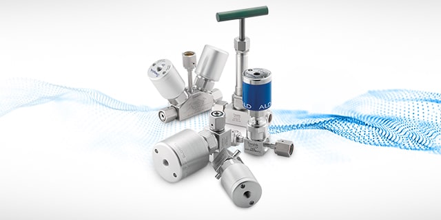
Another consideration that must be made in semiconductor ALD system design is material selection. Next-generation precursors can be highly corrosive to non-compatible materials, meaning system designers must be intentional when sourcing critical components like valves. Even the smallest particles have the potential to be catastrophic for the semiconductor manufacturing process.
Even the smallest particles have the potential to be catastrophic for the semiconductor manufacturing process.
This is especially true of today’s advanced nodes, with small feature sizes that can be more easily compromised. For these reasons, valves and components made from alternative materials (Hastelloy, for example) that are less susceptible to premature deterioration are increasingly necessary for extended valve service life and system uptime.
***
Semiconductor professionals face multifaceted challenges in today’s landscape, and success will continue to depend on collaboration, innovation, and continuous learning—and at Swagelok, we’re ready to help. We have the experience and expertise semiconductor professionals require, and we’re committed to sharing our insights, as well as our complete suite of high-performance components for the most demanding semiconductor applications, with professionals everywhere.
Push your semiconductor processes further. Talk to Swagelok.
Read More Semiconductor Articles
Overcoming ALD Process Challenges
Addressing critical challenges in advanced semiconductor fabrication